Printed circuit boards (PCBs) are the backbone of modern electronics, and their performance and reliability are crucial for the success of any electronic device. One key factor that significantly impacts PCB performance is copper thickness. Thicker copper layers can dramatically enhance thermal management, current-carrying capacity, and overall durability of PCBs. This improvement in performance is particularly critical in high-power applications, where heat dissipation and current handling are paramount concerns.
As electronic devices become more powerful and compact, the demands on PCBs continue to increase. Engineers and designers are constantly seeking ways to optimize PCB performance without compromising reliability or increasing costs significantly. Thick copper PCBs have emerged as a solution to many of these challenges, offering a range of benefits that can make a substantial difference in the functionality and lifespan of electronic devices.
Copper thickness standards in PCB manufacturing
In the world of PCB manufacturing, copper thickness is typically measured in ounces (oz) per square foot. This measurement refers to the weight of copper that would cover one square foot of the board’s surface. Standard PCBs often use 1 oz copper, which translates to approximately 35 micrometers (μm) in thickness. However, thick copper PCBs can range from 2 oz (70 μm) up to 20 oz (700 μm) or even more in extreme cases.
The choice of copper thickness depends on various factors, including the intended application, current requirements, thermal considerations, and mechanical stress. For instance, a standard consumer electronics device might use 1 oz copper, while a high-power LED lighting system could require 3 oz or more. Heavy copper PCB manufacturer specializes in producing boards with copper thicknesses exceeding the standard 1 oz, catering to applications that demand superior performance.
It’s important to note that copper thickness standards are not arbitrary. They are governed by industry specifications such as those set by the IPC (Institute for Printed Circuits). These standards ensure consistency and reliability across different manufacturers and applications. When designing PCBs with thick copper, engineers must consider these standards to ensure compatibility and manufacturability.
Thermal management enhancements with thick copper
One of the most significant advantages of thick copper in PCBs is its ability to enhance thermal management. As electronic devices become more powerful and compact, heat dissipation becomes a critical challenge. Thick copper layers can dramatically improve a PCB’s ability to distribute and dissipate heat, leading to cooler operation and increased reliability.
Heat dissipation in High-Power applications
In high-power applications, such as power supplies, motor controllers, and high-intensity LED systems, heat generation is a major concern. Thick copper layers act as efficient heat spreaders, quickly conducting heat away from hot components and distributing it across the board. This heat-spreading effect can reduce the peak temperature of critical components by up to 30% compared to standard copper thicknesses.
For example, a 5 oz copper layer can dissipate heat approximately five times more effectively than a standard 1 oz layer. This improved thermal performance allows for higher power densities and can often eliminate the need for additional heat sinks or cooling systems, leading to more compact and cost-effective designs.
Thermal conductivity of IMS vs. FR-4 PCBs
When comparing thermal management solutions, it’s essential to consider the differences between Insulated Metal Substrate (IMS) PCBs and traditional FR-4 boards with thick copper. IMS boards, which typically use aluminum as a base material, offer excellent thermal conductivity but can be more expensive and have limitations in terms of layer count and via structures.
Thick copper FR-4 boards, on the other hand, provide a balance between cost and thermal performance. While not as thermally conductive as IMS, thick copper FR-4 boards can still offer significant improvements in heat dissipation compared to standard PCBs. For instance, a 4 oz copper FR-4 board can provide thermal conductivity up to 10 times better than a standard 1 oz board, bridging the gap between traditional FR-4 and IMS solutions.
Copper coin technology for localized heat sinking
For applications requiring intense localized cooling, copper coin technology can be integrated with thick copper PCBs. Copper coins are solid copper inserts that are embedded into the PCB, providing extremely high thermal conductivity in specific areas. This technique is particularly useful for cooling high-power components such as power amplifiers or processors.
Copper coins can be combined with thick copper layers to create a highly effective thermal management system. For example, a 10 oz copper coin embedded in a 3 oz copper PCB can provide thermal resistance as low as 0.2°C/W, which is comparable to some dedicated heat sink solutions.
Thermal vias and their role in heat transfer
Thermal vias play a crucial role in enhancing heat transfer in multilayer PCBs. These are plated through-holes that conduct heat from one layer to another, effectively creating a three-dimensional heat dissipation network. When combined with thick copper layers, thermal vias become even more effective at managing heat.
In a thick copper PCB, thermal vias can be filled with copper, further improving their thermal conductivity. A typical arrangement might include an array of copper-filled vias underneath a high-power component, connected to thick copper planes on inner and outer layers. This configuration can reduce the thermal resistance by up to 50% compared to unfilled vias in standard copper thickness boards.
Current carrying capacity and voltage drop reduction
Another significant advantage of thick copper PCBs is their increased current-carrying capacity and reduced voltage drop. These improvements are particularly valuable in power electronics and high-current applications where efficient power distribution is critical.
Ampacity calculations for thick copper traces
Ampacity, or the maximum amount of electric current a conductor can carry before sustaining immediate or progressive deterioration, increases with copper thickness. The relationship between copper thickness and ampacity is not linear, but it is substantial. For instance, doubling the copper thickness from 1 oz to 2 oz doesn’t just double the ampacity—it can increase it by a factor of 1.8 to 2.2, depending on other factors like trace width and ambient temperature.
Engineers can use specialized calculators or refer to standards like IPC-2152 to determine the appropriate trace width and copper thickness for a given current requirement. For example, a 100-mil wide trace in 2 oz copper can safely carry about 7 amps, while the same width in 4 oz copper can handle over 11 amps, assuming a 10°C temperature rise.
IPC-2152 standard for Current-Carrying capacity
The IPC-2152 standard, titled “Standard for Determining Current-Carrying Capacity in Printed Board Design,” provides comprehensive guidelines for calculating the current-carrying capacity of PCB traces. This standard takes into account factors such as copper thickness, trace width, temperature rise, and board construction.
According to IPC-2152, the current-carrying capacity of a trace increases approximately with the square root of its thickness. This means that a 4 oz copper trace can carry about twice the current of a 1 oz trace of the same width, all other factors being equal. This relationship allows designers to significantly increase current-carrying capacity without proportionally increasing board size, which is crucial for high-power density applications.
Minimizing resistive losses in power distribution networks
Thick copper layers are particularly beneficial in power distribution networks (PDNs) where minimizing resistive losses is crucial. The resistance of a copper trace is inversely proportional to its cross-sectional area. By increasing the copper thickness, the resistance of power planes and traces can be significantly reduced, leading to lower voltage drops and power losses.
For example, in a typical server backplane where currents can exceed 100 amps, using 6 oz copper instead of 2 oz can reduce voltage drop by more than 60%. This reduction in voltage drop not only improves efficiency but also ensures more stable voltage levels across the board, which is critical for the proper operation of sensitive components.
Mechanical strength and durability improvements
Beyond electrical and thermal benefits, thick copper PCBs also offer enhanced mechanical strength and durability. This improved robustness is particularly valuable in applications subject to vibration, thermal cycling, or mechanical stress.
The increased copper thickness provides greater structural integrity to the PCB. This added strength can prevent issues such as trace cracking, pad lifting, and via failure that can occur in standard PCBs under harsh conditions. For instance, a 3 oz copper PCB can withstand significantly more flex cycles before failure compared to a 1 oz board, making it suitable for applications in automotive, aerospace, and industrial environments where reliability under stress is paramount.
Moreover, thick copper layers can act as a heat spreader, reducing thermal gradients across the board. This more even distribution of heat reduces thermal stress and can extend the lifespan of both the PCB and the components mounted on it. In some cases, the use of thick copper can eliminate the need for additional mechanical support structures, leading to simpler and more cost-effective designs.
Electromagnetic interference (EMI) shielding properties
Thick copper layers in PCBs can also contribute significantly to electromagnetic interference (EMI) shielding. As electronic devices become more compact and operate at higher frequencies, managing EMI becomes increasingly important to ensure proper functionality and comply with regulatory standards.
Skin effect and frequency considerations
When dealing with high-frequency signals, the skin effect becomes a significant factor. This phenomenon causes current to flow primarily near the surface of a conductor. For standard PCB copper thicknesses, this can lead to increased resistance and power loss at high frequencies.
Thick copper layers provide more “skin” for high-frequency currents to flow, effectively reducing the AC resistance of traces and planes. For instance, at 1 GHz, the skin depth in copper is approximately 2.1 μm. A 4 oz (140 μm) copper layer provides ample thickness to accommodate this skin effect, ensuring efficient high-frequency performance.
Faraday cage principles in PCB design
Thick copper layers can be used to create effective Faraday cages within the PCB structure. A Faraday cage is an enclosure that blocks electromagnetic fields, and this principle can be applied on a PCB level to isolate sensitive circuits or contain noisy components.
By using thick copper planes and strategically placed vias, designers can create shielding structures that significantly reduce EMI. For example, a sensitive analog circuit can be surrounded by thick copper walls connected to ground planes, effectively creating a mini Faraday cage within the PCB. This technique is particularly useful in mixed-signal designs where digital noise must be kept away from sensitive analog components.
Grounding techniques for EMI reduction
Effective grounding is crucial for EMI reduction, and thick copper layers can greatly enhance grounding strategies. Thick ground planes provide lower impedance paths for return currents, reducing ground bounce and improving signal integrity.
In multilayer PCBs, thick copper ground planes can be placed between signal layers to provide shielding and improve signal integrity. This technique, known as ground sandwiching, is particularly effective when combined with proper stackup design. For instance, a 6-layer board with 2 oz copper ground planes sandwiching 1 oz signal layers can provide excellent EMI performance while maintaining good signal integrity.
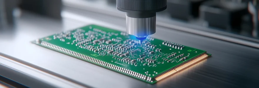
Manufacturing challenges and solutions for thick copper PCBs
While thick copper PCBs offer numerous benefits, they also present unique manufacturing challenges that require specialized processes and expertise to overcome.
Etching precision and undercut control
One of the primary challenges in manufacturing thick copper PCBs is achieving precise etching while controlling undercut. As copper thickness increases, the etching process becomes more difficult to control, potentially leading to issues with trace width consistency and impedance control.
Advanced etching techniques, such as differential etching rates and custom etchants, are employed to maintain precision. For example, a step etching process might be used, where the copper is removed in stages, allowing for better control of the final trace profile. Additionally, specialized imaging processes ensure that the etch resist can withstand the longer etching times required for thick copper.
Plating uniformity in high aspect ratio vias
Plating vias in thick copper boards presents another significant challenge, especially when dealing with high aspect ratio vias (i.e., vias with a high depth-to-diameter ratio). Ensuring uniform copper plating throughout the via is crucial for reliability and electrical performance.
To address this, manufacturers use advanced plating techniques such as pulse plating and reverse pulse plating. These methods provide better control over the plating process, allowing for more uniform copper deposition even in small, deep vias. For extremely high aspect ratio vias, laser drilling combined with specialized plating processes may be employed to achieve the required plating thickness and uniformity.
Impedance control with thick copper layers
Maintaining precise impedance control becomes more challenging with thick copper layers due to the increased copper thickness’s effect on trace geometry and dielectric spacing. The thicker copper can lead to trapezoidal trace profiles, which affect impedance calculations.
To achieve accurate impedance control, manufacturers use advanced modeling software that accounts for the actual trace profile rather than assuming a rectangular cross-section. Additionally, techniques such as copper balancing , where copper thickness is adjusted on different layers to maintain consistent overall thickness, may be employed to achieve the desired impedance values.
Stackup design considerations for mixed copper weights
Designing PCB stackups with mixed copper weights presents unique challenges in terms of maintaining overall board flatness and managing thermal expansion. Uneven copper distribution can lead to warping or twisting of the board during the manufacturing process or under thermal stress.
To mitigate these issues, designers must carefully consider the copper distribution across all layers. Techniques such as copper balancing, where thick copper layers are mirrored on opposite sides of the board’s center, can help maintain flatness. Additionally, the use of high-Tg (glass transition temperature) materials can improve the board’s ability to withstand the thermal stresses associated with thick copper processing.